Product information
Bonding System EHB-400
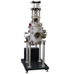
Overview
The EHB-400 is a bonding system for the development of MEMS, sensors, SOI devices, etc.
This system is used for the purpose of high-precision bonding of the same or different materials at the wafer-level. Under a high vacuum environment, performs heating, weighting, substrate cleaning, and alignment can be possible.
Combined with our unique multi-sputtering system, this bonding system can carry out consistent processing in vacuum from multilayer film formation to bonding.
Product specifications
1.A various size of wafer-level (up to 4inch) bonding are compatible.
2.The temperature is accurately controlled by a unique heating mechanism to perform heating and cooling.
3.A surface treatment mechanism using a radical source or ion source can be installed.
4.By connecting with a multi-target sputtering system, it is possible to deposit and form multi-layered films such as metals and oxides.
5.A surface analysis chamber can be added as an option.
